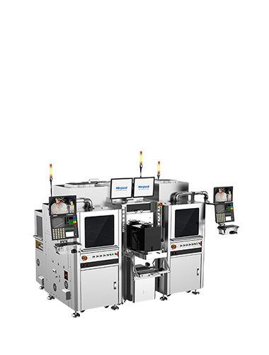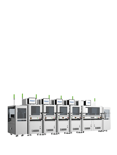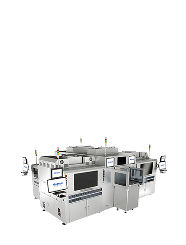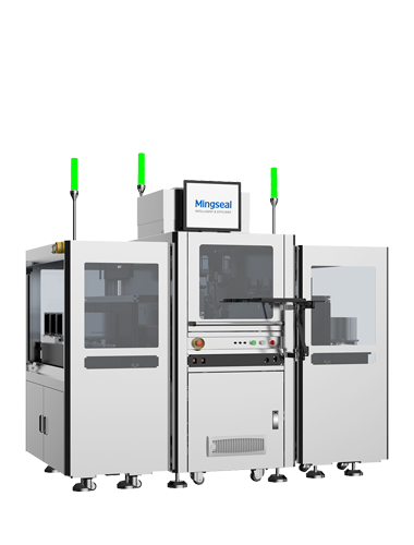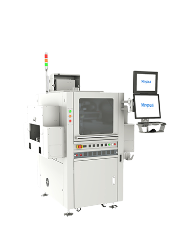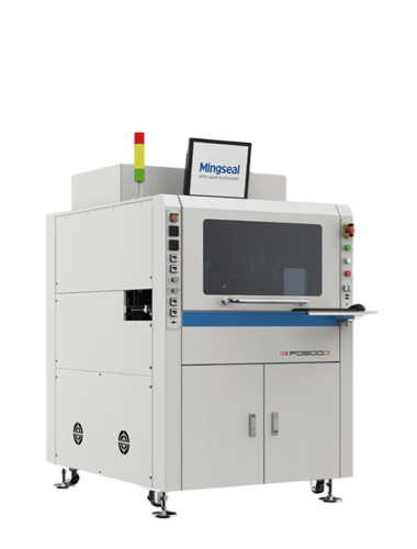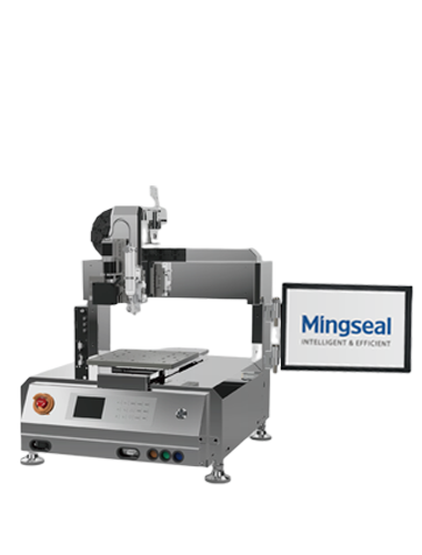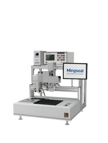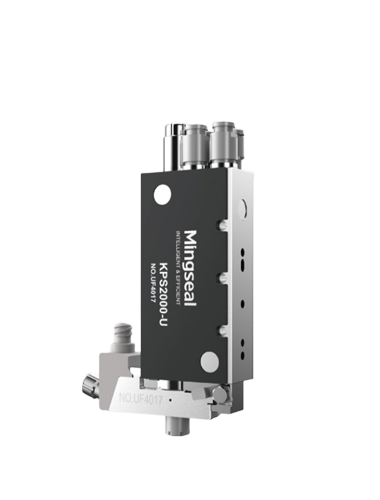
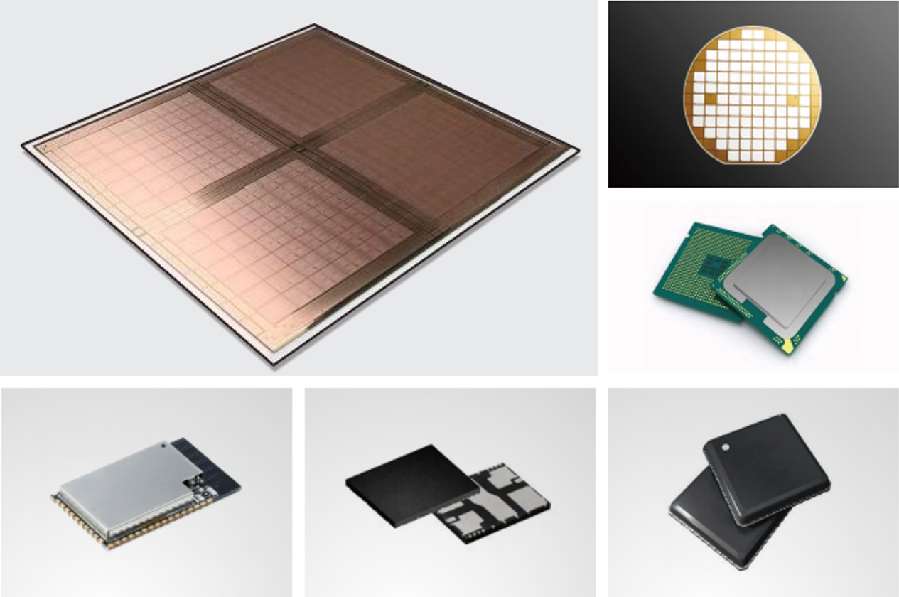
Mainly used in the field of integrated circuit packaging, including wafer-level package (WLP), panel-level package (PLP), flip-chip ball grid array (FCBGA), flip-chip chip scale package (FCCSP) and system-in-package (SiP), etc. Including processes such as Underfill, Dam & Fill, Flux Spray, Solder Paste Painting and Lid Attach.
PLP
WLP
FCBGA
FCCSP
SiP
Underfill
Dam&Fill
Flux Spray
Solder paste painting
Lid Attach
Indium Attach
Ring Attach


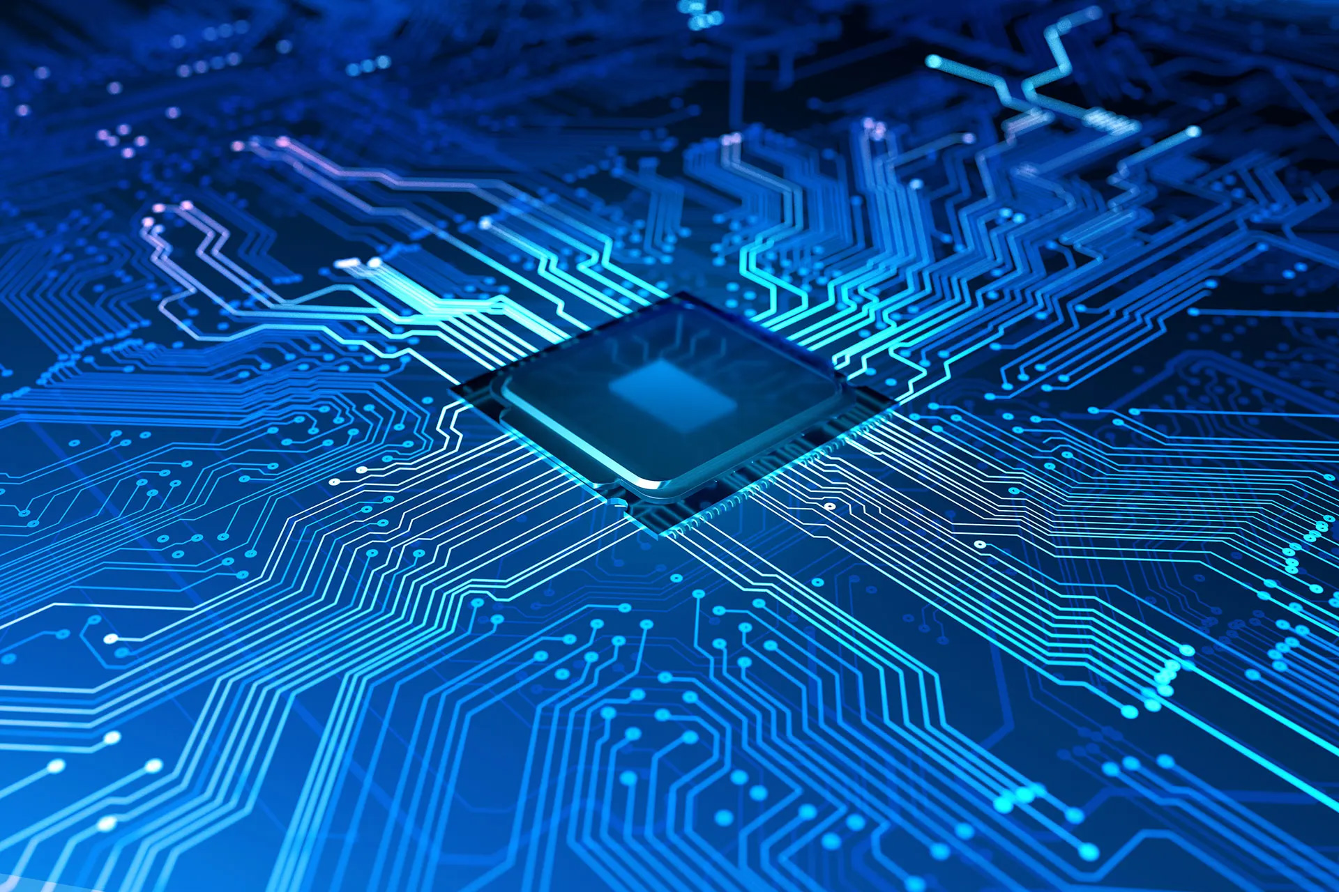
As the core material of third-generation semiconductors, SiC is rapidly replacing traditional silicon devices with its high energy efficiency and miniaturization advantages. With its high hardness and excellent thermal conductivity, SiC is difficult to process using traditional methods that balance both precision and efficiency. Water jet guided laser machining technology, featuring non-contact cutting, efficient cooling, superior surface quality, environmental friendliness, and strong adaptability, enables precise processing of SiC materials. It effectively minimizes the heat-affected zone, prevents material deformation and performance degradation, and ensures the reliability and stability of high-performance devices.
Typical Applications |
Typical Materials |
|---|---|
|
|
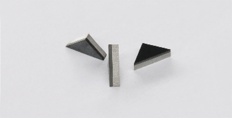 Carbon-based Diamond
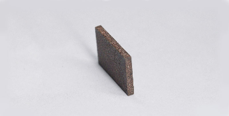 Copper-based Diamond
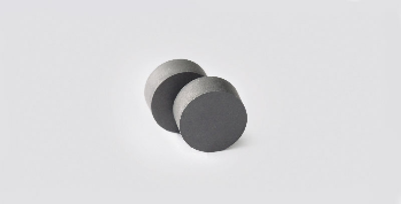 Boron Nitride
 Alumina Ceramic